 | –≠–ª–µ–∫—Ç—Ä–æ–Ω–Ω—ã–π –∫–æ–º–ø–æ–Ω–µ–Ω—Ç: VN771K | –°–∫–∞—á–∞—Ç—å:  PDF PDF  ZIP ZIP |
1/21
September 2004
VN771K-E
QUAD SMART POWER SOLID STATE RELAY
FOR COMPLETE H BRIDGE CONFIGURATIONS
Rev. 1
Table 1. General Features
Note: (*) Total resistance of one side in bridge configuration.
Note: (**) Typical current limitation value.
s
SUITED AS LOW VOLTAGE BRIDGE
s
LINEAR CURRENT LIMITATION
s
VERY LOW STAND-BY POWER DISSIPATION
s
SHORT CIRCUIT PROTECTED
s
STATUS FLAG DIAGNOSTIC (OPEN DRAIN)
s
INTEGRATED CLAMPING CIRCUITS
s
UNDERVOLTAGE PROTECTION
s
ESD PROTECTION
s
IN COMPLIANCE WITH THE 2002/95/EC
EUROPEAN DIRECTIVE
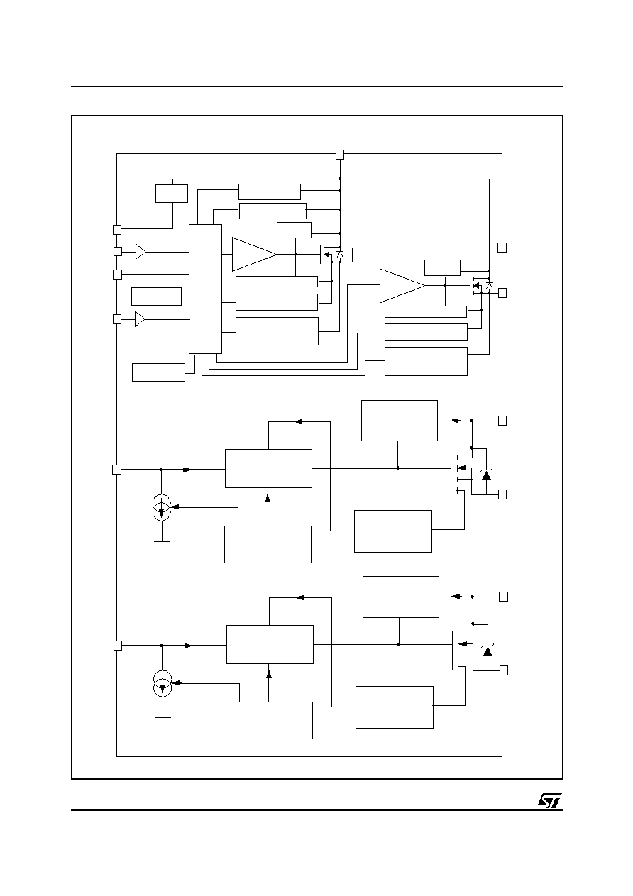
DESCRIPTION
The VN771K-E is a device formed by three
monolithic chips housed in a standard SO-28
package: a double high side and two low side
switches. Both the double high side and low side
switches are made using
|
STMicroelectronics
VIPower
TM
M0-3 Technology. This device is
suitable to drive a DC motor in a bridge
configuration as well as to be used as a quad
switch for any low voltage application.
Figure 1. Package
The dual high side switches have built-in thermal
shutdown to protect the chips from
overtemperature and current limiter blocks to
protect the device from short circuit. Status output
is provided to indicate open load in off and on state
and overtemperature. The low side switches are
two OMNIFET II types (fully autoprotected Power
MOSFET in VIPowerTM technology). They have
built-in thermal shutdown, linear current limitation
and overvoltage clamping. Fault feedback for
thermal intervention can be detected by
monitoring the voltage at the input pin.
Table 2. Order Codes
Type
R
DS(on)
I
OUT
V
CC
VN771K-E
95m
(*)
9A (**)
36V
SO-28
Package
Tube
Tape and Reel
SO-28
VN771K-E
VN771KTR-E
VN771K-E
2/21
Figure 2. Block Diagram
OVERTEMP. 1
V
cc
GND
INPUT1
SOURCE1
OVERVOLTAGE
LOGIC
DRIVER 1
DIAG
V
cc
CLAMP
UNDERVOLTAGE
CLAMP 1
OPENLOAD ON 1
CURRENT LIMITER 1
OPENLOAD OFF 1
SOURCE2
DRIVER 2
CLAMP 2
OPENLOAD ON 2
OPENLOAD OFF 2
OVERTEMP. 2
INPUT2
CURRENT LIMITER 2
Overvoltage
Gate
Linear
DRAIN3
SOURCE3
Clamp
Current
Limiter
Control
Over
Temperature
INPUT3
Overvoltage
Gate
Linear
DRAIN4
SOURCE4
Clamp
Current
Limiter
Control
Over
Temperature
INPUT4
3/21
VN771K-E
Table 3. Pin Function
Figure 3. Configuration Diagram (Top View)
Table 4. Thermal Data
No
NAME
FUNCTION
1, 3, 25, 28
DRAIN 3
Drain of Switch 3 (low-side switch)
2
INPUT 3
Input of Switch 3 (low-side switch)
4, 11
N.C.
Not Connected
5, 10, 19, 24
V
CC
Drain of Switches 1 and 2 (high-side switches) and Power Supply Voltage
6
GND
Ground of Switches 1 and 2 (high-side switches)
7
INPUT 1
Input of Switch 1 (high-side switches)
8
DIAGNOSTIC
Diagnostic of Switches 1 and 2 (high-side switches)
9
INPUT 2
Input of Switch 2 (high-side switch)
12, 14, 15, 18 DRAIN 4
Drain of switch 4 (low-side switch)
13
INPUT 4
Input of Switch 4 (low-side switch)
16, 17
SOURCE 4
Source of Switch 4 (low-side switch)
20, 21
SOURCE 2
Source of Switch 2 (high-side switch)
22, 23
SOURCE 1
Source of Switch 1 (high-side switch)
26, 27
SOURCE 3
Source of Switch 3 (low-side switch)
Symbol
Parameter
Value
Unit
R
thj-case
Thermal Resistance Junction-case
(High-side switch)
MAX
20
∞C/W
R
thj-case
Thermal Resistance Junction-case
(Low-side switch)
MAX
20
∞C/W
R
thj-amb
Thermal Resistance Junction-ambient
MAX
60
∞C/W
VN771K-E
4/21
ABSOLUTE MAXIMUM RATINGS
Table 5. Dual High Side Switch
Table 6. Low Side Switch
Symbol
Parameter
Value
Unit
V
CC
DC Supply Voltage
41
V
- V
CC
Reverse DC Supply Voltage
- 0.3
V
- I
GND
DC Reverse Ground Pin Current
- 200
mA
I
OUT
DC Output Current
Internally Limited
A
- I
OUT
Reverse DC Output Current
- 6
A
I
IN
DC Input Current
+/- 10
mA
I
STAT
DC Status Current
+/- 10
mA
V
ESD
Electrostatic Discharge (Human Body Model: R=1.5K
;
C=100pF)
- INPUT
- STATUS
- OUTPUT
- V
CC
4000
4000
5000
5000
V
V
V
V
P
tot
Power Dissipation T
c
=25∞C
6
W
T
j
Junction Operating Temperature
Internally Limited
∞C
T
c
Case Operating Temperature
- 40 to 150
∞C
T
stg
Storage Temperature
- 55 to 150
∞C
Symbol
Parameter
Value
Unit
V
DS
Drain-source Voltage (V
IN
=0V)
Internally Clamped
V
V
IN
Input Voltage
Internally Clamped
V
I
IN
Input Current
+/-20
mA
R
IN MIN
Minimum Input Series Impedance
10
I
D
Drain Current
Internally Limited
A
I
R
Reverse DC Output Current
-15
A
V
ESD1
Electrostatic Discharge (R=1.5K
, C=100pF)
4000
V
V
ESD2
Electrostatic Discharge on output pin only (R=330
,
C=150pF)
16500
V
P
tot
Total Dissipation at T
c
=25∞C
6
W
T
j
Operating Junction Temperature
Internally limited
∞C
T
c
Case Operating Temperature
Internally limited
∞C
T
stg
Storage Temperature
-55 to 150
∞C
5/21
VN771K-E
ELECTRICAL CHARACTERISTICS FOR DUAL HIGH SIDE SWITCH
(8V<V
CC
<36V; -40∞C< T
j
<150∞C, unless otherwise specified) (Per each channel)
Table 7. Power Outputs
Note:
(1)
Per device.
Table 8. Switching (V
CC
=13V)
Table 9. Logic Input
Table 10. Status Pin
Symbol
Parameter
Test Conditions
Min
Typ
Max
Unit
V
CC
(
1
)
Operating Supply Voltage
5.5
13
36
V
V
USD
(
1
)
Undervoltage Shut-down
3
4
5.5
V
V
OV
(
1
) Overvoltage
Shut-down
36
V
R
ON
On State Resistance
I
OUT
=2A; T
j
=25∞C
I
OUT
=2A; V
CC
> 8V
60
120
m
m
I
S
(
1
)
Supply Current
Off State; V
CC
=13V; V
IN=
V
OUT
=0V
Off State; V
CC
=13V; T
j
=25∞C;
V
IN=
V
OUT
=0V
On State; V
CC
=13V
12
12
5
40
25
7
µ
A
µ
A
mA
I
L(off1)
Off State Output Current
V
IN
=V
OUT
=0V; V
CC
=36V; T
j
=125∞C
0
50
µ
A
I
L(off2)
Off State Output Current
V
IN
=0V; V
OUT
=3.5V
-75
0
µ
A
I
L(off3)
Off State Output Current
V
IN
=V
OUT
=0V; Vcc=13V; T
j
=125∞C
5
µ
A
I
L(off4)
Off State Output Current
V
IN
=V
OUT
=0V; Vcc=13V; T
j
=25∞C
3
µ
A
Symbol
Parameter
Test Conditions
Min
Typ
Max
Unit
t
d(on)
Turn-on Delay Time
R
L
=6.5
from V
IN
rising edge to
V
OUT
=1.3V
30
µ
s
t
d(off)
Turn-off Delay Time
R
L
=6.5
from V
IN
falling edge to
V
OUT
=11.7V
30
µ
s
dV
OUT
/
dt
(on)
Turn-on Voltage Slope
R
L
=6.5
from V
OUT
=1.3V to
V
OUT
=10.4V
See
relative
diagram
V/
µ
s
dV
OUT
/
dt
(off)
Turn-off Voltage Slope
R
L
=6.5
from V
OUT
=11.7V to
V
OUT
=1.3V
See
relative
diagram
V/
µ
s
Symbol
Parameter
Test Conditions
Min
Typ
Max
Unit
V
IL
Input Low Level
1.25
V
I
IL
Low Level Input Current
V
IN
= 1.25V
1
µ
A
V
IH
Input High Level
3.25
V
I
IH
High Level Input Current
V
IN
= 3.25V
10
µ
A
V
I(hyst)
Input Hysteresis Voltage
0.5
V
V
ICL
Input Clamp Voltage
I
IN
= 1mA
I
IN
= -1mA
6
6.8
-0.7
8
V
V
Symbol
Parameter
Test Conditions
Min
Typ
Max
Unit
V
STAT
Status Low Output Voltage I
STAT
= 1.6 mA
0.5
V
I
LSTAT
Status Leakage Current
Normal Operation; V
STAT
= 5V
10
µ
A
C
STAT
Status Pin Input
Capacitance
Normal Operation; V
STAT
= 5V
100
pF
V
SCL
Status Clamp Voltage
I
STAT
= 1mA
I
STAT
= - 1mA
6
6.8
-0.7
8
V
V